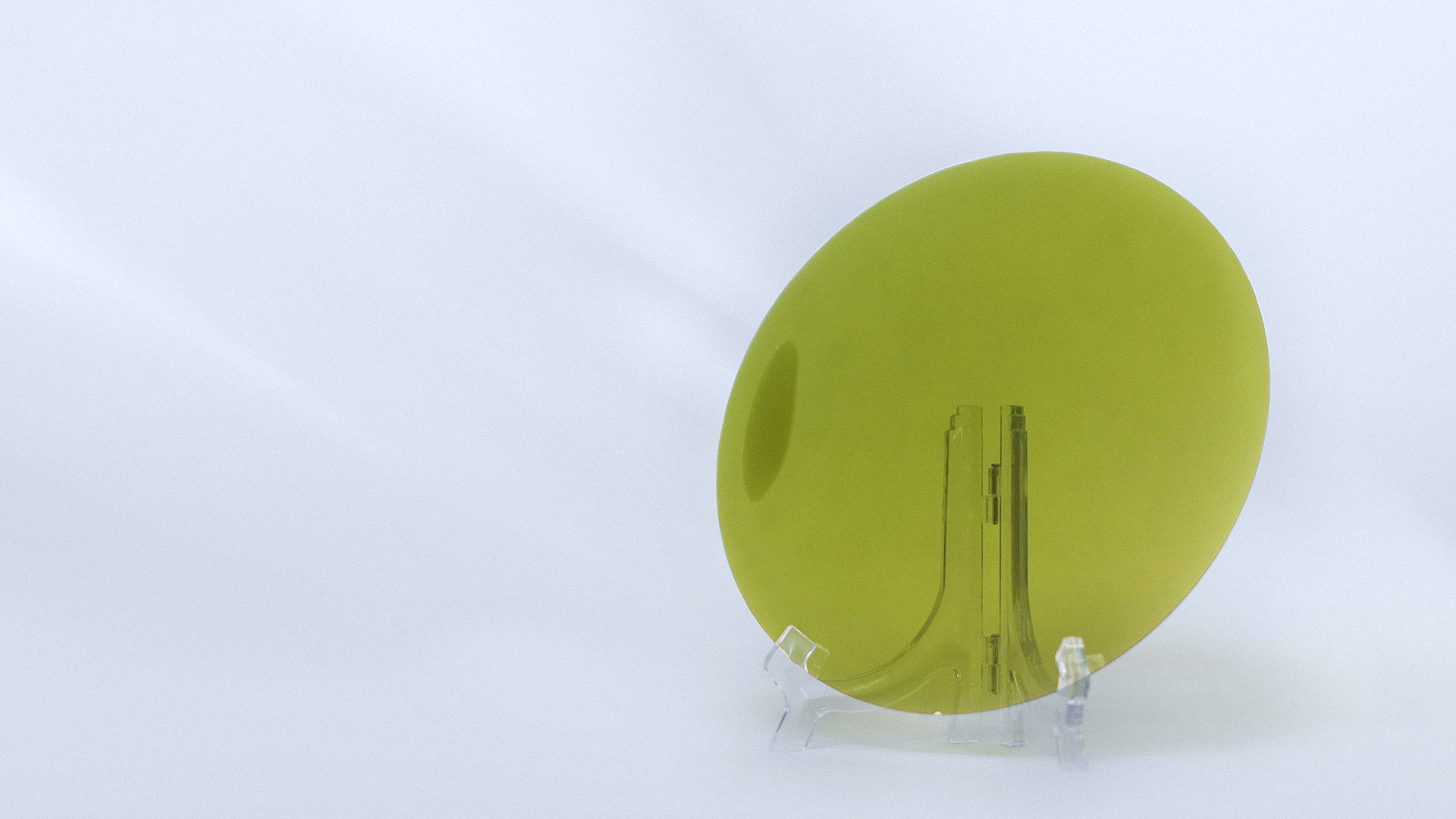
Conductive SiC substrate is a monocrystalline formed by conductive SiC crystal processing through cutting, grinding, polishing, cleaning and other processes. As an important raw material for the third-generation semiconductors, monocrystalline substrate wafers can be made into SiC based power devices after homogeneous epitaxial growth, wafer manufacturing, packaging and testing and other processes.
8-inch conductive substrates are the mainstream size products in the next generation industry. The quality of 8-inch products is equivalent to that of 6-inch products. In the future, the Company will expand the production scale of 8-inch substrates according to actual needs of customer, and effectively reduce production costs to promote the continuous development of 8-inch substrates.
SiC substrate materials are made into SiC diodes, SiC MOSFET and other power devices after homogeneous epitaxial growth, wafer manufacturing, packaging and testing, and other processes. They are suitable for high temperature, high voltage, high current and other working environments, and are widely used in new energy vehicles, charging piles, photovoltaic wind power, energy storage, rail transit, smart grid, industrial power supply, industrial drive, white goods and other fields.


| Diameter | 199.5 mm - 200.0 mm | |
| Poly-type | 4H | |
| Thickness | 500 μm ± 25 μm | |
| Wafer Orientation | 4.0° toward < 11-20 > ± 0.5° | |
| Micropipe Density | ≤ 0.2 cm-2 | |
| Resistivity | 0.015-0.025 Ω.cm | |
| Notch Orientation | {10-10} ± 5.0° | |
| Edge Exclusion | 3 mm | |
| LTV / TTV / Bow / Warp | ≤ 5 μm/≤ 10 μm/ ± 35 μmm/ 70 μm | |
| Roughness | Polish Ra ≤ 1 nm | |
| CMP Ra ≤ 0.2 nm | ||
| Edge Cracks By High Intensity Light | - | |
| Hex Plates By High Intensity Light | Cumulative area ≤ 0.05% | |
| Polytype Areas By High Intensity Light | - | |
| Visual Carbon Inclusions | Cumulative area ≤ 0.05% | |
| Silicon Surface Scratches By High Intensity Light | - | |
| Edge Chips By High Intensity Light | None permitted ≥ 0.2 mm width and depth | |
| Threading screw dislocation | ≤ 300cm-2 | |
| Silicon Surface Contamination By High Intensity Light | - | |
| Packaging | Multi-wafer Cassette Or Single Wafer Container | |
| Diameter | 199.5 mm - 200.0 mm | |
| Poly-type | 4H | |
| Thickness | 500 μm ± 25 μm | |
| Wafer Orientation | 4.0° toward < 11-20 > ± 0.5° | |
| Micropipe Density | ≤ 5 cm-2 | |
| Resistivity | 0.015-0.028 Ω.cm | |
| Notch Orientation | {10-10} ± 5.0° | |
| Edge Exclusion | 3 mm | |
| LTV / TTV / Bow / Warp | ≤ 10 μm/ ≤15 μm/ ± 50 μmm/ 100 μm | |
| Roughness | Polish Ra ≤ 1 nm | |
| CMP Ra ≤ 0.5 nm | ||
| Edge Cracks By High Intensity Light | Cumulative length ≤ 30 mm Single length ≤ 2 mm |
|
| Hex Plates By High Intensity Light | Cumulative area ≤ 0.1% | |
| Polytype Areas By High Intensity Light | Cumulative area ≤ 3% | |
| Visual Carbon Inclusions | Cumulative area ≤ 3% | |
| Silicon Surface Scratches By High Intensity Light | Cumulative length ≤1 × wafer diameter | |
| Edge Chips By High Intensity Light | 9 allowed, ≤ 1 mm each | |
| Threading screw dislocation | - | |
| Silicon Surface Contamination By High Intensity Light | - | |
| Packaging | Multi-wafer Cassette Or Single Wafer Container | |
-
8 Inch Conductive SiC Substrate Specification.pdfDownload


