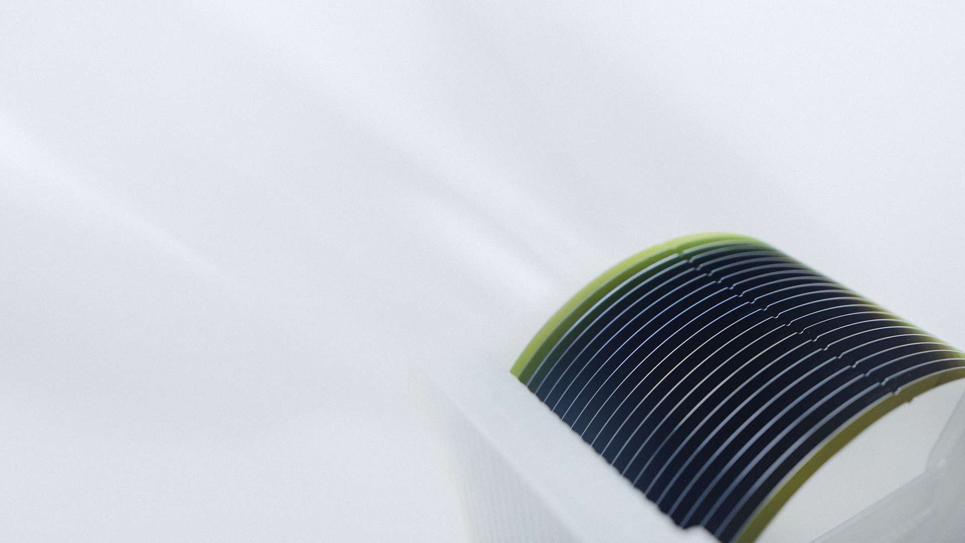
8-inch Conductive Epi-wafer
Technical Achievements
Control technics for low intrinsic concentration less than 1E14 cm-3
Control technics for thickness uniformity less than 3%
Control technics for concentration uniformity less than 6%
Low dislocation control technics, and up to 99% or more of BPD conversion efficiency
Low surface defects control technics with surface defect density of less than 0.2 defects /cm2
Product Overview
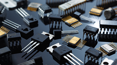
SiC Epi-wafer is made from a layer of high-quality SiC single crystal thin film grown on the self-made SiC substrate using SiC epitaxial equipment. After wafer manufacturing, packaging, testing and other processes, SiC Epi-wafers can be made into SiC power devices.
Downstream Products and Applications
SiC Epi-wafers are made into SiC diodes, SiC MOSFET and other power devices after homogeneous epitaxial growth, wafer manufacturing, packaging and testing, and other processes. They are suitable for high temperature, high voltage, high current and other working environments, and are widely used in new energy vehicles, charging piles, photovoltaic wind power, energy storage, rail transit, smart grid, industrial power supply, industrial drive, white goods and other fields.