High-quality conductive SiC seed wafers are grown by PVT method. They are processed into high-quality SiC single crystals after a series of processes such as rolling the outer circle, grinding the end faces, and processing the flats. Monocrystalline ingots are important raw materials for processing and producing substrates. Customers can obtain SiC single crystal substrate products with low defect density after cutting, grinding, polishing, and other processing processes and cleaning processes.
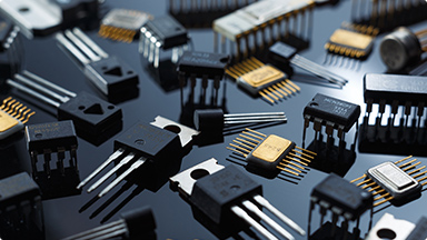
SiC substrate materials are made into SiC diodes, SiC MOSFET and other power devices after homogeneous epitaxial growth, wafer manufacturing, packaging and testing, and other processes. They are suitable for high temperature, high voltage, high current and other working environments, and are widely used in new energy vehicles, charging piles, photovoltaic wind power, energy storage, rail transit, smart grid, industrial power supply, industrial drive, white goods and other fields.


