6-inch Conductive Substrate
Technical Achievements
Micropipe-free density control technics
Low dislocation density control technics
Low stacking faults density control technics
Resistivity uniformity control technics
Ultra thin substrate processing and flatness control technics
Product Overview
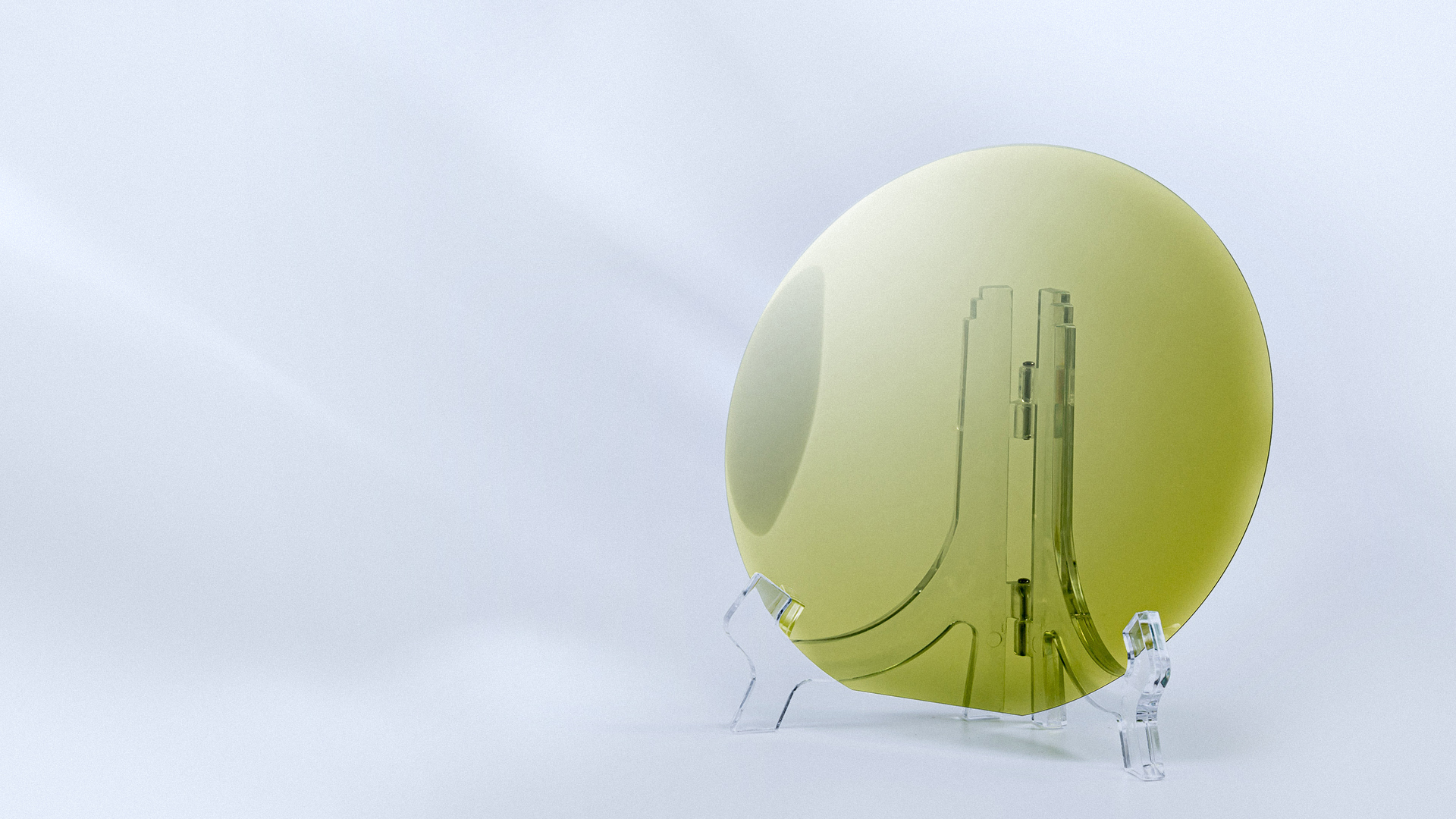
Conductive SiC substrate is a monocrystalline formed by conductive SiC crystal processing through cutting, grinding, polishing, cleaning and other processes. As an important raw material for the third-generation semiconductors, monocrystalline substrate wafers can be made into SiC based power devices after homogeneous epitaxial growth, wafer manufacturing, packaging and testing and other processes. Currently, 6-inch conductive substrates are the mainstream size product in the industry. Our 6-inch conductive substrates have reached international standards in quality and have a very high cost-effectiveness. After comprehensive verification by downstream customers, the product performance is stable and reliable, and significant results have been achieved in automotive grade and industrial applications.
Downstream Products and Applications
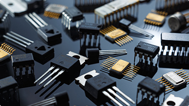
SiC substrate materials are made into SiC diodes, SiC MOSFET and other power devices after homogeneous epitaxial growth, wafer manufacturing, packaging and testing, and other processes. They are suitable for high temperature, high voltage, high current and other working environments, and are widely used in new energy vehicles, charging piles, photovoltaic wind power, energy storage, rail transit, smart grid, industrial power supply, industrial drive, white goods and other fields.


Substrate Specification
| Diameter | 149.5 mm - 150.0 mm | |
| Poly-type | 4H | |
| Thickness | 350 μm ± 15 μm | |
| Wafer Orientation | Off axis : 4.0° toward < 11-20 > ±0.5° | |
| Micropipe Density | ≤ 0.2 cm-2 | |
| Resistivity | 0.015-0.024 Ω·cm | |
| Primary Flat Orientation | {10-10} ± 5.0° | |
| Primary Flat Length | 47.5 mm ± 2.0 mm | |
| Edge Exclusion | 3 mm | |
| LTV / TTV / Bow / Warp | ≤ 2.5 μm/ ≤6 μm/ ≤ 25 μm/ ≤ 35 μm | |
| Roughness | Polish Ra ≤ 1 nm | |
| CMP Ra ≤ 0.2 nm | ||
| Edge Cracks By High Intensity Light | - | |
| Hex Plates By High Intensity Light | Cumulative area ≤ 0.05% | |
| Polytype Areas By High Intensity Light | - | |
| Visual Carbon Inclusions | Cumulative area ≤ 0.05% | |
| Silicon Surface Scratches By High Intensity Light | - | |
| Edge Chips High By Intensity Light | None permitted ≥ 0.2 mm width and depth | |
| Threading Screw Dislocation | ≤ 500 cm-2 | |
| Silicon Surface Contamination By High Intensity Light | - | |
| Packaging | Multi-wafer Cassette Or Single Wafer Container | |
| Diameter | 149.5 mm - 150.0 mm | |
| Poly-type | 4H | |
| Thickness | 350 μm ± 15 μm | |
| Wafer Orientation | Off axis : 4.0° toward < 11-20 > ±0.5° | |
| Micropipe Density | ≤ 15 cm-2 | |
| Resistivity | 0.015-0.028 Ω·cm | |
| Primary Flat Orientation | {10-10} ± 5.0° | |
| Primary Flat Length | 47.5 mm ± 2.0 mm | |
| Edge Exclusion | 3 mm | |
| LTV / TTV / Bow / Warp | ≤ 5 μm/ ≤ 15 μm/ ≤ 40 μm/ ≤ 60 μm | |
| Roughness | Polish Ra ≤ 1 nm | |
| CMP Ra ≤ 0.5 nm | ||
| Edge Cracks By High Intensity Light |
Cumulative length ≤ 20 mm Single length ≤ 2 mm |
|
| Hex Plates By High Intensity Light | Cumulative area ≤ 0.1% | |
| Polytype Areas By High Intensity Light | Cumulative area ≤ 3% | |
| Visual Carbon Inclusions | Cumulative area ≤ 3% | |
| Silicon Surface Scratches By High Intensity Light | Cumulative length ≤1 × wafer diameter | |
| Edge Chips High By Intensity Light | 7 allowed, ≤ 1 mm each | |
| Threading Screw Dislocation | - | |
| Silicon Surface Contamination By High Intensity Light | - | |
| Packaging | Multi-wafer Cassette Or Single Wafer Container | |
Documents
-
6 Inch Conductive SiC Substrate Specification.pdfDownload