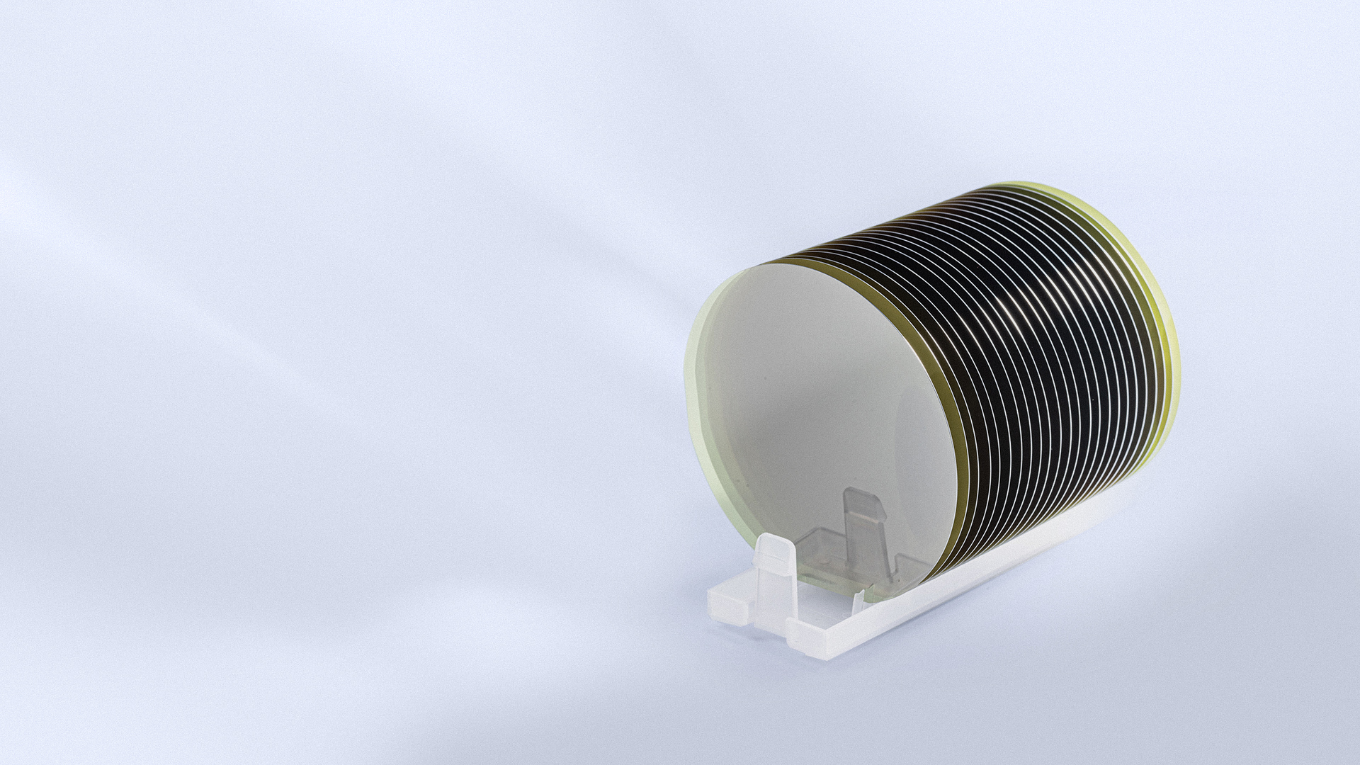
Conductive SiC substrate is a monocrystalline formed by conductive SiC crystal processing through cutting, grinding, polishing, cleaning and other processes. As an important raw material for the third-generation semiconductors, monocrystalline substrate wafers can be made into SiC based power devices after homogeneous epitaxial growth, wafer manufacturing, packaging and testing, and other processes. They are important foundational materials for the development of the third-generation semiconductor industry. To meet the diverse needs of customers for small-sized products, we still retain the production capacity for small-sized products of 4 inches and below to ensure worry-free supply.
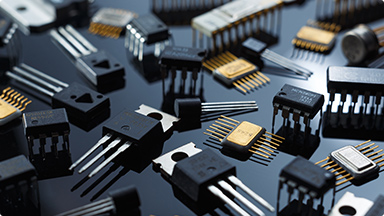
SiC substrate materials are made into SiC diodes, SiC MOSFET and other power devices after homogeneous epitaxial growth, wafer manufacturing, packaging and testing and other processes. They are suitable for high temperature, high voltage, high current and other working environments, and are widely used in new energy vehicles, charging piles, photovoltaic wind power, energy storage, rail transit, smart grid, industrial power supply, industrial drive, white goods and other fields.


| Diameter | 99.5 mm - 100.0 mm | |
| Poly-type | 4H | |
| Thickness | 350 μm ± 15 μm | |
| Wafer Orientation | Offaxis : 4.0°toward < 11-20 > ± 0.5° | |
| Micropipe | ≤ 0.2 cm-2 | |
| Resistivity | 0.015-0.024 Ω·cm | |
| Primary Flat Orientation | {10-10} ± 5.0° | |
| Primary Flat Length | 32.5 mm ± 2.0 mm | |
| Secondary Flat Length | 18.0 mm ± 2.0 mm | |
| Secondary Flat Orientation | Silicon face up: 90° CW. from Prime flat± 5.0° | |
| Edge Exclusion | 3 mm | |
| LTV / TTV / Bow / Warp | ≤2.5 μm/ ≤ 5 μm/ ≤ 15 μm/ ≤ 30 μm | |
| Roughness | Polish Ra ≤ 1 nm | |
| CMP Ra ≤ 0.2 nm | ||
| Edge Cracks By High Intensity Light | - | |
| Hex Plates By High Intensity Light | Cumulative area ≤ 0.05% | |
| Polytype Areas By High Intensity Light | - | |
| Visual Carbon Inclusions | Cumulative area ≤ 0.05% | |
| Silicon Surface Scratches By High Intensity Light | - | |
| Edge Chips High By Intensity Light | None permitted ≥ 0.2 mm width and depth | |
| Silicon Surface Contamination By High Intensity | - | |
| Threading Screw Dislocation | ≤ 500cm-2 | |
| Packaging | Multi-wafer Cassette Or Single Wafer Container | |
| Diameter | 99.5 mm - 100.0 mm | |
| Poly-type | 4H | |
| Thickness | 350 μm ± 25 μm | |
| Wafer Orientation | Offaxis : 4.0°toward < 11-20 > ± 0.5° | |
| Micropipe | ≤ 15 cm-2 | |
| Resistivity | 0.015 -0.028 Ω·cm | |
| Primary Flat Orientation | {10-10} ± 5.0° | |
| Primary Flat Length | 32.5 mm ± 2.0 mm | |
| Secondary Flat Length | 18.0 mm ± 2.0 mm | |
| Secondary Flat Orientation | Silicon face up: 90° CW. from Prime flat± 5.0° | |
| Edge Exclusion | 3 mm | |
| LTV / TTV / Bow / Warp | ≤ 10 μm/ ≤ 15 μm/ ≤ 25 μm/ ≤ 40 μm | |
| Roughness | Polish Ra ≤ 1 nm | |
| CMP Ra ≤ 0.5 nm | ||
| Edge Cracks By High Intensity Light |
Cumulative length ≤ 10 mm Single length ≤ 2 mm |
|
| Hex Plates By High Intensity Light | Cumulative area ≤ 0.1% | |
| Polytype Areas By High Intensity Light | Cumulative area ≤ 3% | |
| Visual Carbon Inclusions | Cumulative area ≤ 3% | |
| Silicon Surface Scratches By High Intensity Light | Cumulative length ≤1 × wafer diameter | |
| Edge Chips High By Intensity Light | 5 allowed, ≤ 1 mm each | |
| Silicon Surface Contamination By High Intensity | - | |
| Threading Screw Dislocation | - | |
| Packaging | Multi-wafer Cassette Or Single Wafer Container | |
-
4 Inch Conductive SiC Substrate Specification.pdfDownload


