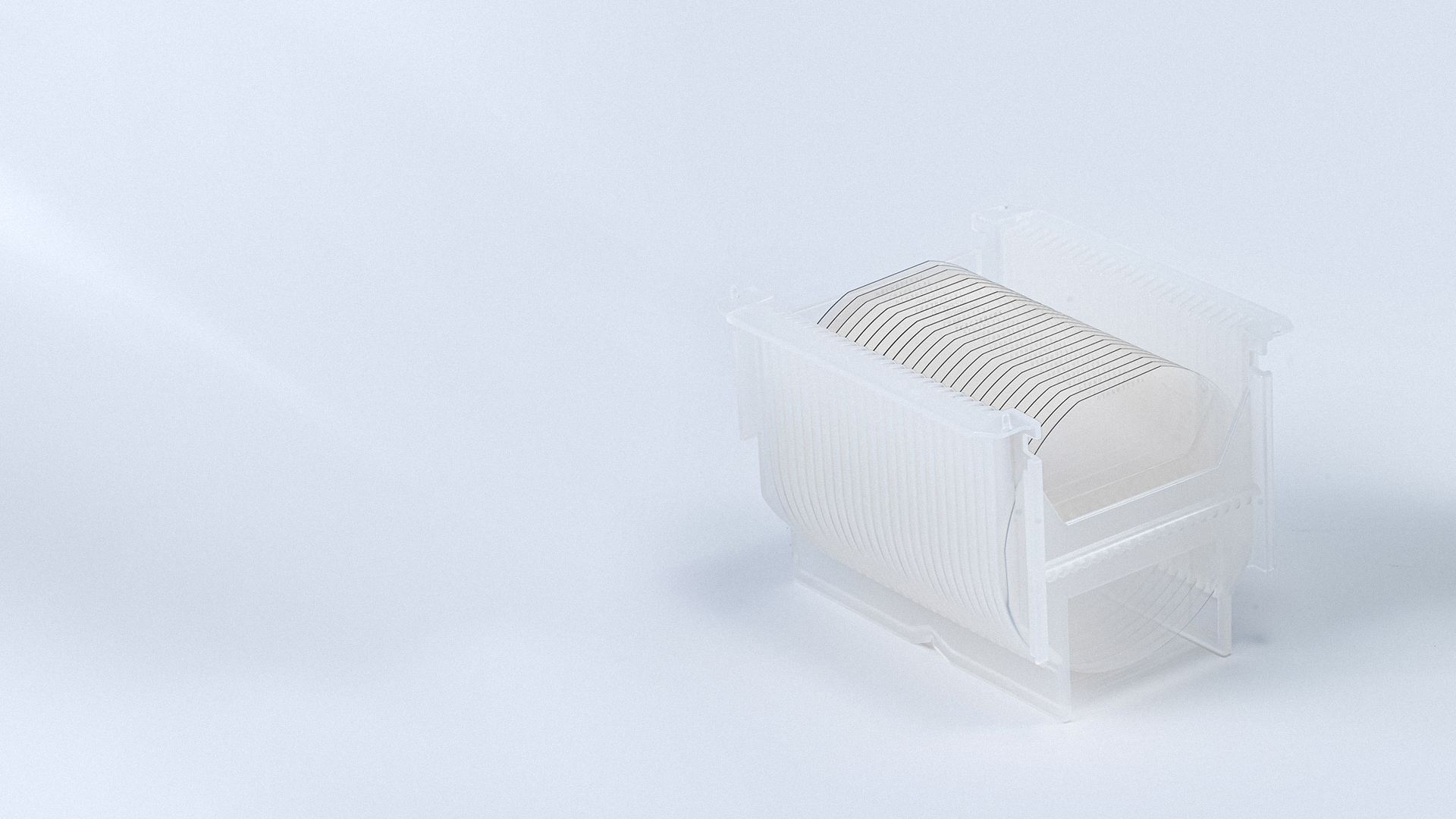
Semi-insulating SiC substrate is a monocrystalline formed by semi-insulated SiC crystal processing through cutting, grinding, polishing, cleaning and other processes. As an important raw material for the third-generation semiconductors, monocrystalline substrate wafers can be made into SiC based RF devices through heteroepitaxial growth, device manufacturing and other processes. They are important foundational materials for the development of the third-generation semiconductor industry. To meet the demand of customers for 4-inch products, TanKeBlue provides 4-inch semi-insulating substrates with high cost-effectiveness for domestic and foreign customers in batches
By growing gallium nitride heteroepitaxial layers on semi-insulated SiC substrates, SiC based gallium nitride epitaxial wafers are obtained. Through wafer manufacturing, packaging and testing, microwave RF devices can be further made, mainly used in the RF field, such as 5G communication, phased array radar, and wireless electrical detectors.


| Diameter | 99.5 mm - 100.0 mm | |
| Poly-type | 4H | |
| Thickness | 500 μm ± 15 μm | |
| Wafer Orientation | On axis : <0001> ± 0.5° | |
| Micropipe | ≤ 1 cm-2 | |
| Resistivity | ≥1E10 Ω.com | |
| Primary Flat Orientation | {10-10} ± 5.0° | |
| Primary Flat Length | 32.5 mm ± 2.0 mm | |
| Secondary Flat Length | 18.0 mm ± 2.0 mm | |
| Secondary Flat Orientation | Silicon face up: 90° CW. from Prime flat ± 5.0° | |
| Edge Exclusion | 3 mm | |
| LTV / TTV / Bow / Warp | ≤ 2.5 μm/ ≤ 5 μm/ ≤ 15 μm/ ≤ 30 μm | |
| Roughness | Polish Ra ≤ 1 nm | |
| CMP Ra ≤ 0.2 nm | ||
| Edge Cracks By High Intensity Light | - | |
| Hex Plates By High Intensity Light | Cumulative area ≤ 0.05% | |
| Polytype Areas By High Intensity Light | - | |
| Visual Carbon Inclusions | Cumulative area ≤ 0.05% | |
| Silicon Surface Scratches By High Intensity Light | - | |
| Edge Chips High By Intensity Light | None permitted ≥ 0.2 mm width and depth | |
| Silicon Surface Contamination By High Intensity | - | |
| Packaging | Multi-wafer Cassette Or Single Wafer Container | |
| Diameter | 99.5 mm - 100.0 mm | |
| Poly-type | 4H | |
| Thickness | 500 μm ± 25 μm | |
| Wafer Orientation | On axis : <0001> ± 0.5° | |
| Micropipe | ≤ 15 cm-2 | |
| Resistivity | ≥1E5 Ω.com | |
| Primary Flat Orientation | {10-10} ± 5.0° | |
| Primary Flat Length | 32.5 mm ± 2.0 mm | |
| Secondary Flat Length | 18.0 mm ± 2.0 mm | |
| Secondary Flat Orientation | Silicon face up: 90° CW. from Prime flat ± 5.0° | |
| Edge Exclusion | 3 mm | |
| LTV / TTV / Bow / Warp | ≤ 10 μm/ ≤ 15 μm/ ≤ 25 μm/ ≤ 40 μm | |
| Roughness | Polish Ra ≤ 1 nm | |
| CMP Ra ≤ 0.2 nm | ||
| Edge Cracks By High Intensity Light |
Cumulative length ≤ 10 mm Single length ≤ 2 mm |
|
| Hex Plates By High Intensity Light | Cumulative area ≤ 0.01% | |
| Polytype Areas By High Intensity Light | Cumulative area ≤ 3% | |
| Visual Carbon Inclusions | Cumulative area ≤ 3% | |
| Silicon Surface Scratches By High Intensity Light | Cumulative length ≤1 × wafer diameter | |
| Edge Chips High By Intensity Light | 5 allowed, ≤ 1 mm each | |
| Silicon Surface Contamination By High Intensity | - | |
| Packaging | Multi-wafer Cassette Or Single Wafer Container | |
-
4 Inch Semi-Insulating SiC Substrate Specification.pdfDownload


